Of all the choices in digital cameras, few are as fundamental as the type of image sensor: Complementary Metal Oxide Semiconductor (CMOS) or Charge Coupled Device (CCD). Both types have their adherents, and both have advantages. At Sony, we care passionately about every aspect of image sensor technology. And we’re extremely partial to… both. As a world leader in image sensors, we manufacture both in roughly equal numbers. This puts us in an ideal position to comment on how the two compare.
A look at CCDs.
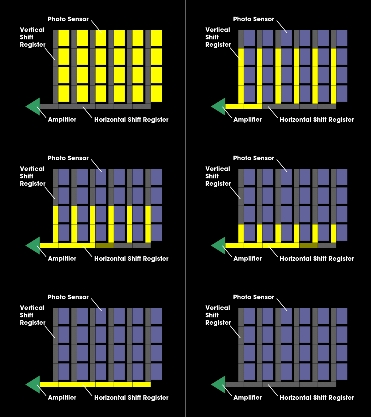
CCD and CMOS technologies have been vying for image sensor supremacy for decades. CCD seized the early lead for high-quality applications largely on the basis of low noise. A CCD is essentially a big array of semiconductor “buckets” that can convert incoming photons into electrons and hold the accumulated charge. In the Interline Transfer CCD design, some buckets are exposed to the light and accumulate charge during the exposure time. Other buckets are hidden behind opaque surfaces and form shift registers that serve to transfer charges. Vertical shift registers move the buckets of charge to one or more horizontal shift registers, which end at specialized buckets that convert the charge to voltage.

Simplified GIF animation of a CCD image sensor with Interline Transfer technology. After the buckets of charge accumulate in the individual photo sensors, they are simultaneously transferred into the vertical shift registers. Buckets of charge move down the vertical registers and across the horizontal register. At the end, charge is converted to voltage and amplified.
Seeing CMOS.
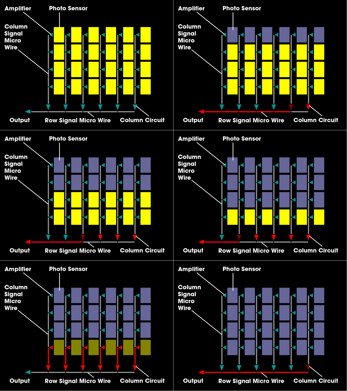
The refinement of high-quality active pixel CMOS image sensors has brought this sensor type to new prominence. Instead of transporting buckets of charge, the Complementary Metal Oxide Semiconductor design immediately converts the charge to voltage and outputs the voltage on micro wires.

Simplified GIF animation of a CMOS image sensor with active pixel sensor (APS) technology. Where a CCD converts charge to voltage at the end of the process, a CMOS sensor performs this conversion at the outset. The voltages can then be output over compact, energy-saving micro wires.
How the technologies compare.
From webcams and mobile phones to high-end digital cinematography, there’s an overwhelming diversity of image sensors on the market. This makes it easy to find counterexamples to almost any generalization. So we’ll try to tread lightly comparing the two technologies.
- Noise. For decades, CCDs had the advantage, especially in fixed pattern noise. Now both are capable of clean imaging.
- Vertical Smear. This artifact, caused by bright highlights leaking into the vertical shift register, has long been the Achilles Heel of CCDs. However modern CCDs are nearly immune.
- Power Supply. CCDs need higher voltage, consume more power and generate more heat. While these issues are less urgent in shoulder-mount cameras, they make CMOS a more attractive choice in small, handheld cameras.
- Processing Speed. The physical arrangement of CCDs limits them to only a few horizontal shift registers, meaning only a few parallel outputs. CMOS has no such limitation. This enables very high processing speed, important for high pixel counts and/or high frame rates.
- Flexibility. The physical architecture of a CCD puts a strict limit on the way the signal can be offloaded. In CMOS architecture, each photo sensor is individually addressable. You can get almost any imaginable output from the full frame down to an individual pixel. A CMOS camera can offer higher frame rates from a smaller window, or 2.1 megapixel HD output from a 14.2 megapixel DSLR sensor.
- Rolling Shutter Artifacts. CCD enjoys global shutter, meaning that every photo sensor begins and ends exposure simultaneously. Typical CMOS sensors have rolling shutter, where each horizontal row of pixels starts and ends exposure slightly before the next row. This slight offset has no affect on still subjects. But it can distort the geometry of on-screen objects in case of camera or subject motion. Rolling shutter can also trigger flash banding in the presence of camera flash or emergency vehicle strobe lights. In flash banding, the strobe appears in a horizontal band across the screen while areas above and below are not affected. The severity of rolling shutter artifacts vary greatly from scene to scene, as well as from one CMOS sensor design to another.
To see where Sony draws the line between CMOS and CCD, please turn to Page 2.
Where Sony nets out.
Our comprehensive involvement in both cameras and image sensors gives Sony a powerful advantage. Where there’s no image sensor to support a Sony camera program, we can build a new one from scratch. From this vantage point, we increasingly prefer CMOS sensors for smaller, lighter professional cameras, where low power consumption and low heat generation are particularly valuable. We prefer CCDs in large-format cameras where ultimate image quality and geometric accuracy are most important. The dividing line is currently among two-thirds inch shoulder mount cameras, where the PMW-350 uses CMOS sensors, while the PMW-500, PDW-700, PDW-F800, HDW-F900R, SRW-9000 and F23 all use CCDs.
Semiconductors and Sentiment.
Behind the technology of Sony image sensors, there are people. When Willard Boyle and George E. Smith of Bell Labs invented the CCD, Sony was paying complete attention. Reading the first journal article on CCD in 1970, Sony engineers saw the device as a potential solid-state replacement for TV camera pickup tubes. Company president Kazuo Iwama sensed even greater potential and commenced full-scale R & D in 1973.
After twelve years and more than $100 million invested, Sony finally succeeded in mass producing a CCD with 250,000 pixels, the ICX018. In 1985, this was incorporated into Sony’s first 8mm camcorder, the aptly named CCD-V8. Unfortunately, Iwama did not live to see the achievement. To commemorate Iwama’s contribution, his successor, Norio Ohga, took an ICX018 CCD from the first production lot and affixed it to the back of Iwama’s tombstone.
For their achievement inventing the CCD, Boyle and Smith were awarded the Nobel Prize in Physics in 2009. For its role in commercializing the CCD, Iwama’s company went on to become a world leader in both semiconductor image sensors and the cameras that use them.

Filmtools
Filmmakers go-to destination for pre-production, production & post production equipment!
Shop Now


