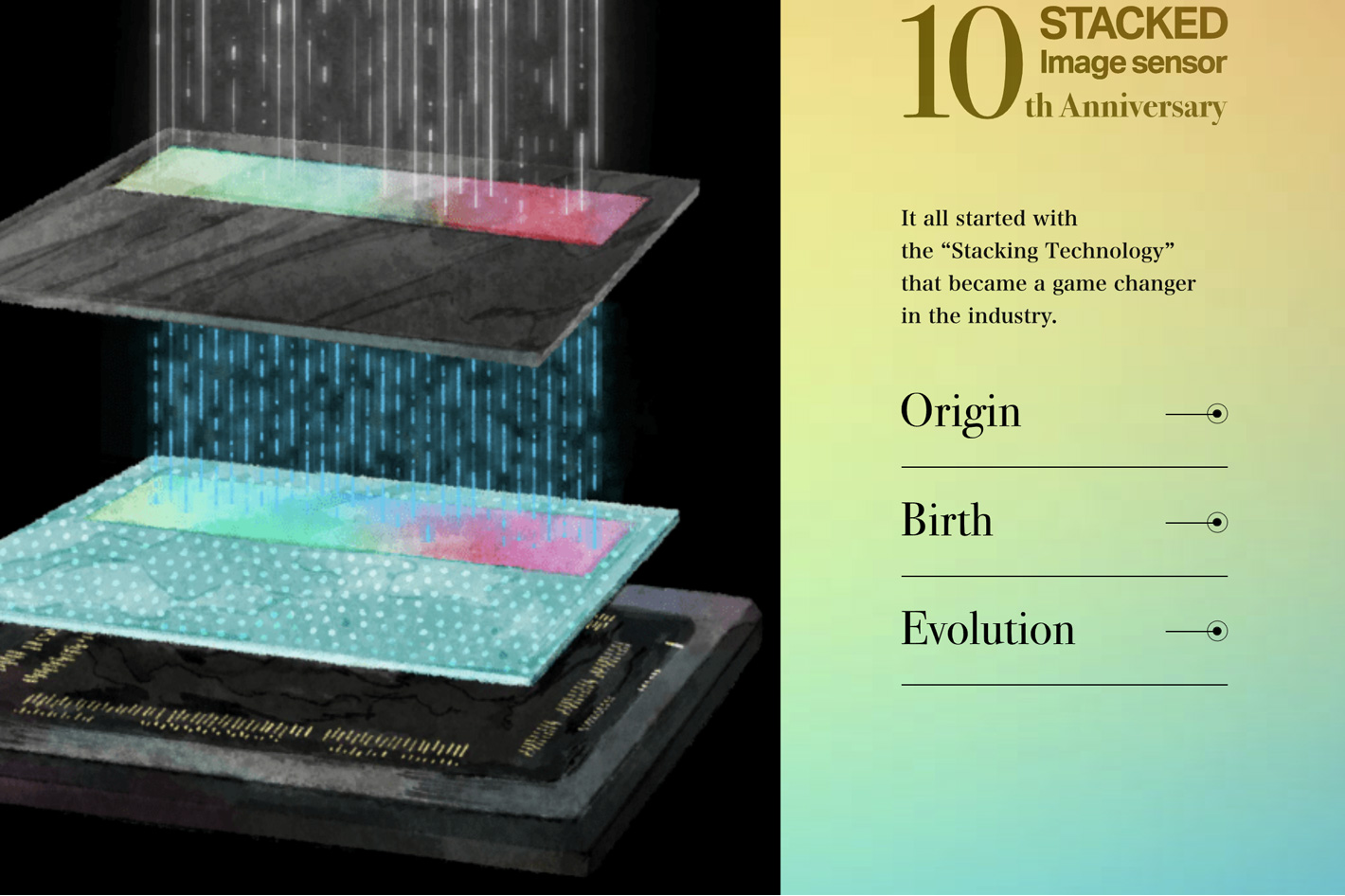
The magic a smartphone camera offers you today would not be possible without the invention of image sensors, those devices that function like the retina in the human eye, capturing light that comes through the camera lens and converts it into electrical signals to form a digital picture. The CCD or “electronic eye”, born in the Spring 1970, offered great potential, but it was the invention of Sony’s “stacked CMOS image sensor”, 10 years ago, that moved the whole industry forward. The stacked CMOS image sensor is prevalent in society today, with smartphones being the most recognizable example.
Sony’s history of image sensor development goes back more than half a century, with the introduction of a CCD image sensor, ICX008, in 1978, adopted in a CCD color camera mounted on a Japanese airline ANA’s jumbo jet. According to Sony, “passengers were thrilled to see the real-time images during a take-off and landing. Dedicated efforts continued by the development and manufacturing teams to improve the production yields, and in 1985 we successfully created the CCD-V8, our consumer 8mm video recorder with a built-in camera.”
Delving, as the company puts it, “in the uncharted path of thorns”, Sony managed, in 1989, to launch the CCD-TR55, an 8mm camcorder that stirred a sensation in the market for its advanced features and smaller size, launched under a copy of “a passport-size camcorder.” This success lifted Sony to the leading position in the image sensor industry.


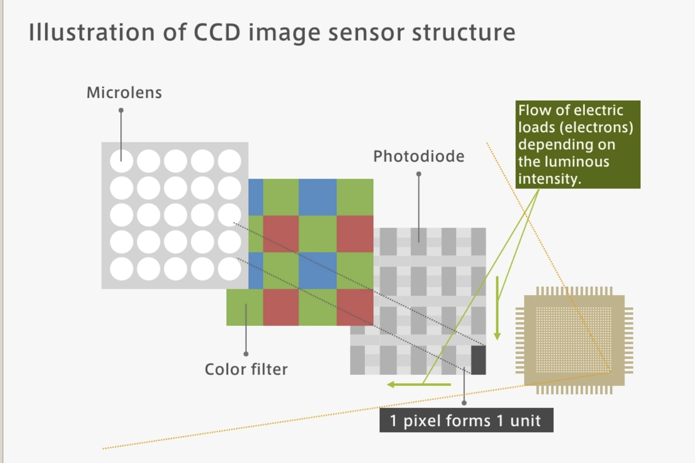
Despite being a leader in the CCD market, Sony decided that the future was elsewhere, and made a critical decision to change its direction towards CMOS image sensors. The advantages were evident: compared to CCD, which forwards the electric signals in a relay, CMOS can transmit the signals much faster due to its structure. Moreover, it works on lower voltage and consumes less power. It was CMOS image sensor that better suited for movies and high-definition imagery. The drawback with the CMOS image sensor was the signal’s susceptibility to noise, as the noise generated in each pixel was amplified concurrently with the signals.
As it happens, Sony was one of the last to join the development of CMOS image sensors, but aware of the fact that CMOS image sensor would be an unavoidable choice in the future, the company discontinued the investment in augmenting the production of CCD image sensors in 2004 and turned its attention to the development of CMOS image sensors.
Despite the problems with the initial CMOS sensors, which helped to make CCDs dominant, Sony understood that CMOS was the future if only there was a way to increment the brightness of the image while reducing the noise. Sony’s engineers believed that the light blockage could be avoided “if we put the photodiode closer to the incident light” but that had never been tried, even though the idea of a back-illuminated structure had been around for nearly two decades.
Sony’s secret investigation
A project started in 2002 inside Sony explored the creation of a back-illuminated CMOS image sensor. It took the team seven long and painful years to develop a commercially viable back-illuminated CMOS image sensor, which was first used in digital high vision camcorders, or “Handycam,” HDR-XR520V and HDR-XR500V.
Excited with the options, the company decided that the next step was to create a back-illuminated CMOS image sensor that could be mounted on a mobile phone camera to deliver the value of this image sensor to more people. The first back-illuminated CMOS image sensor for mobile phones was launched in 2010, but Sony was aware that the image quality was far short of the levels expected of future mobile phone cameras.
The search for a better solution, though, had started a couple of years earlier, in 2008, when a small team at Sony investigated, secretly, the idea of stacked CMOS image sensors. It was only in 2012 that Sony announced the development of its stacked CMOS image sensor. Shipment started in October, after the August launch of the product.
Smartphones are, nowadays, one of the key devices when it comes to the stacking technology. Sony notes that “someone who is not a professional photographer may shoot amazing photos and movies today using a small, slim mobile device, thanks to the features like the 4K imaging, high dynamic range imaging for high-contrast scenes, and AF (autofocus) tracking that automatically keeps a focus on the target even when it is in motion” and adds “today’s smartphones are also equipped, in their compact and slim bodies, with several cameras, from a large aperture to telephoto cameras. This is all thanks to the stacking technology, which has enabled to ultimately minimize the image sensor size, leading to small, high definition, cameras with enhanced capabilities.”
According to a US research firm, Strategy Analytics, the market for CMOS image sensors for mobile applications in 2021 grew 3% year on year to 15.1 billion dollars, and Sony Semiconductor Solutions has the largest share, accounting for 45%.
To read the whole story about the development of CCD and CMOS sensors at Sony, follow the link to the series of articles under the name Stacked Image Sensor 10th Anniversary.

